About Diodes
Diodes
Diodes are usually made from semiconductor materials, Silicon and Germanium being the most common. Early types of semiconductor diodes were made from Selenium and Germanium, but Silicon is used today for the vast majority of devices. Selenium rectifier diodes may be found in antique radios but are obsolete and are normally replaced by modern silicon types. Some germanium types are still used however, because of a number useful properties, which germanium possesses that silicon does not, although specialised types of silicon diodes are taking over uses previously given to germanium diodes.
Figure 3.1.1 c Diodes
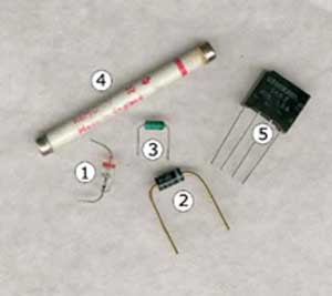
- 1. Germanium point contact diode
- 2. Silicon rectifier
- 3. Silicon high voltage (800V) switching diode
- 4. EHT (20kV) rectifier
- 5. Silicon bridge rectifier

A diode is a one-way conductor. It has two terminals, the anode or positive terminal and the cathode or negative terminal. Basically a diode will only pass current when its anode is made more positive than its cathode.
Which way does current flow?
We say that current then flows from the positive (anode) terminal to the negative (cathode) terminal although in reality current is the movement of electrons in the opposite direction, from cathode to anode.
Conventional current was of course thought of before electrons were discovered and many engineers still use conventional current flow when describing circuit operation, others use electron flow in their descriptions which has current and electrons flowing in the same direction - from negative to positive. To try and minimise confusion we shall attempt to make clear which system we are using when the direction of current flow is being discussed by using the term "conventional current" when we are talking about current flowing from positive to negative. In regard to semiconductor devices we are normally talking about electron flow when describing what goes on inside the device. In many instances however, the direction of the current, conventional or electron flow, doesn´t really make a difference to the description.
Conventional current flow through a diode.

Diodes are the simplest of all the semiconductor devices, but have a very wide range of uses, including -
- • Rectification (changing A.C. power to D.C. power)
- • Demodulation (recovering audio or video information from radio signals)
- • Illumination (light emitting diodes replace filament lamps in many applications)
- • Stabilisation. (Zener diodes can be used to set very precise voltage values in such circuits as d.c. power supplies)
- • Protection (diodes can be used to protect circuits from being damaged by such things as wrong polarity supply connection, and abnormally high voltages or currents)
Diodes are made from a semiconductor material that has two differently doped layers forming a "PN junction". The P type material has a surplus of positive charge carriers (holes) and the N type, a surplus of electrons. Between these layers, where the P type and N type materials meet, holes and electrons combine so that a thin layer is created that has neither positive nor negative charge carriers present.
Since there are no charge carriers in this Depletion Layer no current can flow across it. In effect a small natural potential is set up within the semiconductor material that has an opposite polarity to the P and N type layers and because of this narrow band of reversed potential no current can flow through the diode. When a voltage is applied across the junction however, so that the P type anode is made positive and the N type cathode negative, provided that the applied voltage is greater than the natural junction potential of the depletion layer, the positive holes are attracted across the depletion layer towards the negative cathode, also the negative electrons are attracted towards the positive anode and current flows.
When the diode is reverse biased (the anode connected to negative and the cathode to the positive voltage) the positive holes are attracted towards the negative voltage and away from the junction. Likewise the negative electrons are attracted away form the junction towards the positive voltage applied to the cathode. This action leaves a greater area at the junction without any charge carriers (either positive or negative) left. This causes the depletion layer to widen. It is depleted of charge carriers and so is an insulator. As higher voltages are applied in reverse polarity to the diode the depletion layer becomes wider still since the applied voltage is attracting more charge carriers away from it. The diode will not conduct therefore with a reverse voltage (a reverse bias) applied. Once the voltage is applied in the forward direction (positive to anode and negative to cathode) again, current will flow; in this case as the voltage is increased more current flows. The increase in current does not follow a straight-line relationship, as it would do if we increase the voltage across a resistor however. To begin with no current flows until the applied voltage reaches the "junction potential". Once this is overcome (at about 0.15V for germanium diodes and about 0.6V for silicon) current rises sharply as the diode conducts.
Diode I/V Characteristics
The operation of diodes (as with other semiconductor devices) is often described by a special graph called a "characteristic curve". These graphs show the relationship between the currents and voltages associated with the different terminals of the device. An understanding of these graphs helps in understanding how the device operates.
For diodes the characteristic curve is called an I/V curve because it shows the relationship between the voltage applied between the anode and cathode, and the resulting current flowing through the diode. A typical I/V characteristic is shown in figure 3.1.1e.
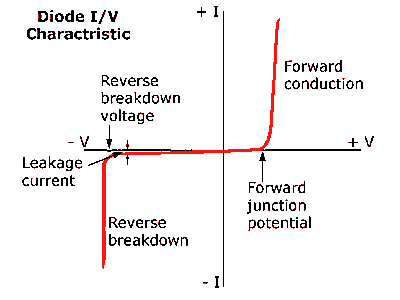
Fig 3.1.1e Typical Diode I/V Characteristic
The axes of the graph show both positive and negative values and so intersect at the centre. The intersection has a value of zero for both current (the Y axis) and voltage (the X axis). The axes +I and +V (top right) show the current rising steeply after an initial zero current area. This is the forward conduction of the diode when the anode is positive and cathode negative. Initially no current flows until the applied voltage is at about the forward junction potential, after which current rises steeply showing that the forward resistance (I/V) of the diode is very low; a small increase in voltage giving a large increase in current.
The -V and -I axes show the reverse biased condition (bottom left). Here we see that although the voltage increases hardly any current flows. This small current is called the leakage current of the diode and is typically only a few micro-amps with germanium diodes and even less in silicon. If a high enough reverse voltage is applied however there is a point (called the reverse breakdown voltage) where the insulation of the depletion layer breaks down and a very high current suddenly flows. In most diodes this breakdown is permanent and a diode subjected to this high reverse voltage will be destroyed. In Zener diodes however, this point is used to give the diode its special ability to stabilise the applied voltage: If the voltage increases at this point heavy current flows and reduces the voltage. The breakdown in a Zener diode is not destructive due to its special construction.