JFET Characterization
Field Effect Transistors
JFETs (Junction Field Effect Transistors)
Although there are lots of confusing names for field effect transistors (FETs) there are basically two main types. The reverse biased PN junction types; the JFET or Junction FET, (these are also called the JUGFET or Junction Unipolar Gate FET), and the insulated gate FET devices (IGFET). All FETs can be called UNIPOLAR devices because the charge carriers that carry the current through the device are all of the same type i.e. either holes or electrons, but not both. This distinguishes FETs from the bipolar devices in which both holes and electrons are responsible for current flow in any one device.
The JFET
This was the earliest FET device available. It is a voltage-controlled device in which current flows from the SOURCE terminal (equivalent to the emitter in a bipolar transistor) to the DRAIN (equivalent to the collector). A VOLTAGE applied between the source terminal and a GATE terminal (equivalent to the base) is used to control the source - drain current. The main difference between a JFET and a bipolar transistor is that in a JFET no gate current flows, the current through the device is controlled by an electric field, hence "Field effect transistor". The JFET construction and circuit symbols are shown in fig 3.1.15a-c.
JFET Construction
The construction of JFETs can be theoretically quite simple, but in reality difficult, requiring very pure materials and clean room techniques. JFETs are made in different forms, some being made as discrete (single) components and others, using planar technology as integrated circuits.
Fig 3.1.15a Diffusion JFET Construction
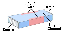
Fig 3.1.15a shows the (theoretically) simplest form of construction for a Junction FET (JFET) using diffusion techniques. It uses a small slab of N type semiconductor into which are infused two P type areas to form the Gate. Current (electrons) flows through the device from source to drain along the N type silicon channel. As only one type of charge carrier (electrons) carry current in N channel JFETs, these transistors are also called "Unipolar" devices.
 Watch it
work with an interactive diagram
Watch it
work with an interactive diagram
Fig 3.1.15b JFET Planar Construction

Fig 3.1.15b shows the cross section of a N channel planar Junction FET (JFET) The load current flows through the device from source to drain along a channel made of N type silicon. In the planar device the second part of the gate is formed by the P type substrate.
P channel JFETs are also available and the principle of operation is the same as the N channel type described here; but polarities of the voltages that are of course reversed and the charge carriers are holes.
Fig 3.1.15c JFET Circuit symbols
