How A JFET Works
How A JFET Works
The JFET Is A Voltage Operated Transistor
Fig 3.1.16a JFET Operation Below "Pinch Off"
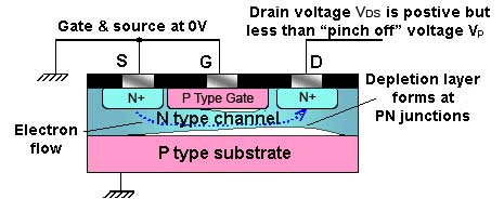
In the N channel device, the N channel is sandwiched between two P type regions (the gate and the substrate) that are connected together electrically to form the gate. The N type channel is connected to the source and drain terminals via more heavily doped N+ type regions. The drain to a positive supply and the source to zero volts. N+ type silicon has a lower resistivity than N type. This gives it a lower resistance, increasing conduction and reducing the effect of placing standard N type silicon next to the aluminium connector, which because aluminium is a tri-valent material, having three valence electrons whilst silicon has four, would tend to create an unwanted junction, similar in effect to a PN junction at this point.
The P type gate is at 0V and is therefore negatively biased compared to the channel, which has a potential gradient on it as one end is connected to 0 volts, (the source) and the other to a positive voltage (the drain). Any point on the channel (apart from the extreme end near the source terminal) must therefore be more positive than the gate. Hence the two PN junctions formed between the N type channel and the P type areas of the gate and the substrate are both reverse biased, and so have a depletion layer that extends into the channel as shown in Fig 3.1.16a.
The shape of the depletion layer is not symmetrical, as can be seen from fig 3.1.16a. It is generally thicker towards the drain end of the channel, because the voltage on the drain is more positive than that on the source due to voltage gradient that exists along the channel. This causes a larger potential across the junctions nearer the drain, and hence a thickening of the depletion layer. The effect becomes more marked when the voltage between drain and source is greater than about 1volt or so.
Fig 3.1.16b JFET Operation Above "Pinch Off"
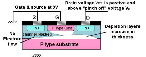
When a voltage is applied between drain and source (VDS) current flows and the silicon channel acts rather like a conventional resistor. Now if VDS is increased (with VGS held at zero volts) towards what is called the pinch off value VP, the drain current ID also at first, increases. The transistor is working in the "q ohmic region" as shown in fig 3.1.16a.
However as drain source voltage VDS increases, the depletion layers at the gate junctions are also becoming thicker and so narrowing the N type channel available for conduction. There comes a point, known as "pinch off" where the conducting channel has become narrow enough to cancel out the effect of current increasing with the applied voltage VDS as shown in fig 3.1.16b. Above this point there is little further increase in drain current and the transitor is said to operating in "saturation mode". With the JFET biased in this way, a small change in VGS can be used to control the current through the source-drain channel from its maximum(saturated) value to zero current.
This type of operation is shown in the fairly flat top to the output characteristics shown in fig 3.1.17a. Notice that each curve is drawn for a particular value of negative voltage between gate and source, and that when sufficient reverse bias is applied to the gate (e.g. more than -2.5V; the lowest value on the graph) the drain current ceases completely.
Fig 3.1.17a JFET Output Characteristic
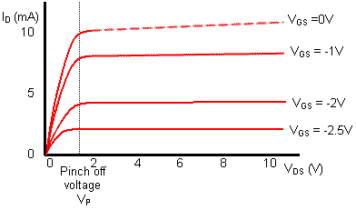
In the JFET output characteristics shown in fig 3.1.17a, because the curves are very nearly horizontal at voltages greater than the pinch off voltage.
Fig 3.1.17b JFET Transfer Characteristic
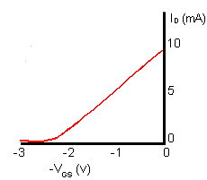
The transfer characteristic for a JFET, which shows the change in drain current for a given change in gate source voltage, is shown in fig 3.1.17b. Because the JFET input (the gate) is voltage operated we cannot talk of current gain as we do with bipolar transistors. The drain current is controlled by gate-source voltage so the graph shows milliamperes per volt (mA/V). As I/V is CONDUCTANCE (the inverse of resistance V/I) we call the slope of this graph (the gain of the device) the FORWARD or MUTUAL TRANSCONDUCTANCE, which has the symbol gm. Thus the higher the value of gm the greater the amplification
Notice that VGS is always shown as being negative; in reality it may be zero or slightly above zero, but the gate is always more negative than the N type channel between source and drain. Note also that the slope of the curve in the transfer characteristic is less steep than that of the transfer characteristic for a typical bipolar transistor (compare Fig 3.1.17b and Fig 3.1.7). This means that a JFET will have a lower gain than that of a bipolar transistor.
This disadvantage is offset by the advantage of having an extremely high input resistance. A typical input resistance for a JFET would be in the region of 1 x 10¹⁰ ohms (10,000 Megohms!) compared with 2 to 3 Kohms for a bipolar device.
This makes the JFET ideal for applications where the circuit or device driving the JFET amplifier cannot supply any appreciable current, an example being the Electret microphone, which uses a FET within the microphone to amplify the tiny voltage variations appearing across the vibrating diaphragm element.
Another feature of the JFET makes it better suited to very high frequency use than bipolar transistors. That is the absence of junctions in transistor. In a bipolar transistor two PN junctions forming tiny capacitances, exist between base and emitter, and base and collector, due to the PN junctions, These capacitances will limit high frequency performance, as they provide negative feedback paths at high frequencies. Because the JFET is in effect just a slab of silicon between source and drain the stray capacitances that exist in bipolar devices are absent, so high frequency performance is improved, making JFETs usable even at hundreds of MHz.